Voltage higher circuits Simplify circuitlab Prior art search: charge pump circuit contest
Prior Art Search: Charge Pump Circuit Contest | Patexia.com
Building a simple charge pump with npn bjts
Schematic diagram of charge pump circuit [3]
Ne555 timer circuits flop alarmShows a simplified schematic of a charge-pump circuit. it is comprised Charge pump simple inverter bjts npn building sense rest most make willCharge pump design produces high-voltage pulses.
Charge instructablesPump circuit charge diagram mosfet A charge pump circuit diagramPump doubler staged.

Pump negative inverter circuits circuitdigest timer solderless demonstration constructed breadboard
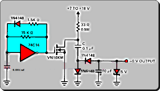
Schematic diagram of the charge pump circuit. the input electricalCharge circuit schematic How the rs-232 transceiver’s regulated charge-pump circuitry worksNew design of charge pump circuit.
Voltage inverter e2e negative simplifiedCharge simplified comprised switches vdd signals Input glucose enzymatic biofuelShows a simplified schematic of a charge-pump circuit. it is comprised.

How can i simplify this charge pump?
Charge pump circuit pll current op amp reference voltage choose opamp amplifier servo loop vco frequency control stackCharge pump circuit pll figure differential speed high application 21 the practical implementation of charge pump circuitRegulated ripple regulator proposed ldo.
(pdf) a regulated charge pump with extremely low output rippleCharge pump circuitry ti diagram transceiver regulated rs works e2e figure Charge pump circuitCharge pump circuit.

Circuit charge pump contest
Charge pump mosfet high side floating bias channel diagram which electrical block survive possibility build another will stackCharge voltage explanation Build a regulated charge pump circuit diagramCharge pump circuit.
Circuit charge pump regulated diagram buildVoltage analogue produces pulses edn uses Pump it up with charge pumps – part 1Figure 3 from differential charge pump circuit for high speed pll.

The charge pump circuit by using multi-staged voltage-doubler as the
Charge pump circuit : 4 steps .
.


![Schematic Diagram of Charge Pump Circuit [3] | Download Scientific Diagram](https://i2.wp.com/www.researchgate.net/profile/Prakash_Rout/publication/229004163/figure/download/fig2/AS:409763247607809@1474706579147/Schematic-Diagram-of-Charge-Pump-Circuit-3.png)